PCBs
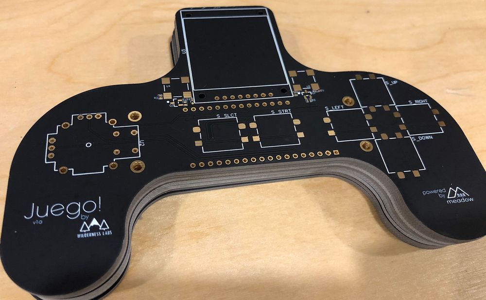
Printed Circuit Boards (PCBs) are the basis of all modern electronics. They provide both a foundation for the electronic components that power a circuit, as well as the wiring, known as traces, that connect them.

PCBs can be created using either a rigid or flexible substrate. Rigid PCBs are most often built with alternating layers of fiberglass and etched copper, but aluminum is also sometimes used. Flexible circuits are often used when a circuit has to bend, such as when attaching a display to a rigid board.
PCB Design Lifecycle
The process of creating a PCB typically consists of the following steps:
- Design - The schematic for the circuit is created, and then the PCB is laid out in Electronic Design Automation (EDA) software.
- Fabrication - Once the PCB design is finished, drawing files known as Gerbers are output and sent to a board fabrication house. A fabrication house will etch the circuit design into the copper layers and place an interconnects, known as vias, through the board, do any necessary routing and cutting, and then cover all the copper that isn't meant to be exposed with solder mask, and then silk screen any designs and labels onto it.
- Assembly - After the PCB has been fabricated, it's ready for assembly, where solder paste is applied to the exposed pads, components are placed, and then the whole thing is heated up until the solder melts and adheres the components to the board.
- Validation - Finally, once the PCB is fully assembled, the design is validated through testing, and if there are any changes to be made, the process starts again.
PCB Design
In the PCB Design Tutorial, you'll learn how to use modern techniques to rapidly design PCBs.
PCB Fabrication
In the PCB Fabrication Guide we'll cover how to take your PCB designs and turn them into PCBs.
PCB Assembly (PCBA) in a Home Lab
While production-scale PCB assembly is done with solder paste stencil printers, pick-and-place machines, reflow ovens, and other specialized equipment, assembling prototype PCBs at home can be done with very simple and cheap tools. In fact, the minimum tooling required to do modern PCB assembly only includes:
- Solder Paste in a Syringe
- Tweezers
- A Hot Plate
In the PCB Assembly tutorial we'll cover everything you need to know to do PCBA at home.
Through Hole (PTH) vs. Surface Mount (SMT/SMD)
An important concept to understand when designing and working with PCBs is the difference between (Plated) Through-Hole (PTH), and Surface Mount Technology/Devices (SMT/SMD).
PTH and SMT refer to how the components are attached to the board.
(Plated) Through-Hole (PTH)
Through-Hole means that the components have leads that are placed through holes in the PCB and then soldered on the back:
[TODO: Need image of PTH]
Surface-Mount-Technology/Devices (SMT/SMD)
Surface-Mount means that instead of going through the PCBs, the component leads actually sit on the surface of the PCB, where they're soldered to pads.
[TODO: image of SMT]
Advantage of SMT/SMD Designs
Most modern PCB designs are primarily SMD because they have a number of advantages over PTH designs, including:
- Machine Assembly - SMD designs can be assembled by a pick-and-place machine and therefore are much cheaper to manufacture.
- Smaller - Surface mount components can be made with very small leads, thereby reducing the overall size of the components which saves space, shortens routing, and enables for much more complex and precise electrical designs.
- Simplified Routing - By only using real estate on one side of the PCB, surface mount components also provide more options for routing underneath then, enabling much more complex circuit designs in a smaller area.
Hybrid Designs
With that said, it's not uncommon for a PCB to mostly use surface mount components, but also have some limited set of through hole devices.